
Welcome to this post about patents and chips. Not a lot has been written about this combination, but there is a lot to know, especially for the innovators and entrepreneurs themselves. In this three-weekly series, I talk about various aspects, from a dual perspective of a patent agent and a semiconductor entrepreneur. If you like the article and read it on LinkedIn, give it a thumbs up, and/or click on Follow. If you like to work with us for your next patent, "contact us" info is on www.icswpatent.com. You can also subscribe/unsubscribe for short email alerts when the next post is available.
|
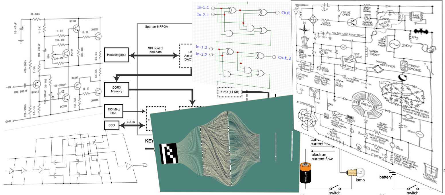
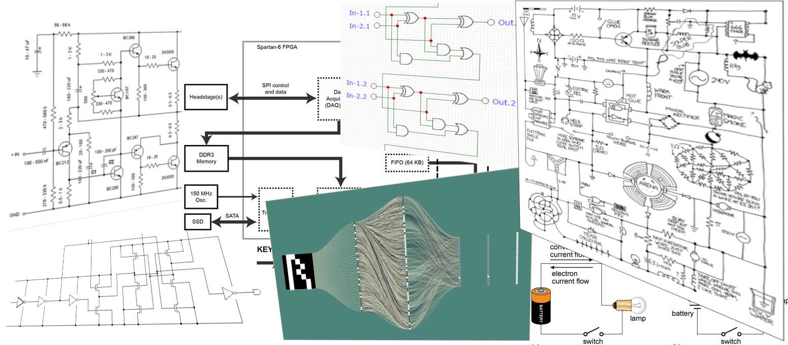
Credits: Julian Jenkins, Brandon Rohrer, xkcd, Justin Kinney et al., deeptronic.com, Open University, and apkpure.com |
One thing that is greatly different between many chip design inventions and most other inventions is that there are so many ways in which you can implement them. Of course, there are some inventions that are only half a transistor different than what was there before. But not many. There are quite a few inventions that focus on the system level, and you can decide to implement one as an analog circuit, a hard-wired digital circuit, a configured digital circuit (e.g., in an FPGA or similar), firmware running in a processor, or yet something else. Additionally, for each of these technologies, there may be fundamentally different architectures that do what's intended, and then different circuits that can do it. And each of these may be physically implemented in potentially an infinite number of ways. In case of a digital implementation, you may not even know what's exactly on silicon, as your silicon compiler generates the circuit for you based on your behavioral language input.
So how many patents do you need to file? One, six, infinite?
Basically one (if you have done what for the patent office counts as one invention). But, you must know and understand exactly what that one invention is. The inventor, usually an engineer, was most likely busy solving a problem when he/she was developing a product. You could decide that his/her solution is the invention, and write an application for it, file it, and get a patent. But most engineers don't have time to fully analyze how broadly their invention could be applied, or how it would look in other technologies than the one that they are using. They know that they have something new, but also that their bosses are breathing down their necks to meet tight schedules and tight budgets. Or their customers are breathing down their necks. They spend their time making their implementation work as well as possible. If you file a patent application that describes just that one solution, then the patent may be way too narrow.
As patent practitioners, we find that writing a robust application for a chip design invention can take as much as 30-40% more time than for other types of applications. The reason is that we have to spend a lot of time deciphering the engineer's language, finding out the information that was missing from the invention disclosure, analyzing the invention, and figuring out all the ways that it could have been implemented other than how it has been implemented. Then we need to document and explain the broadest invention, and describe all the different technologies and architectures and/or circuits in which it can be implemented.
We need to go through that process to avoid that we write a patent that documents and claims one particular implementation, and that teaches or suggests to competitors what the real trick is, allowing them to find their own ways to make another implementation while sidestepping just the one that was claimed. There are many patents out there that have huge gaping holes, enabling competitors. The only thing that stops many engineers from exploiting these holes is that they hate reading the arcane language used in many patents. (And in my experience, the ones with the ugliest language are often also the ones with the biggest holes). But they often do read the IEEE publications that follow or accompany the filing of the patent.
If you're smart, you might decide to find a patent practitioner who writes language that wears one out, especially a competitor of course. If you're smarter, you might decide to find a patent practitioner who writes good patents. Well-written patents can save you tons of money not just during the application phase, but also should it ever get to litigation. Litigators love to squabble over every dot, colon, and comma, and definitely over how things are described. Where you have two eager prize fighters each at $1000 per hour, and their support teams, you can imagine a black hole in your wallet. Perhaps spending a few thousand dollars more for writing a robust application isn't such a bad idea.
So what's your next step?
Have a look at a design that your best inventor patented, any time in the past decade. Look at the drawings. You may first see something that shows some prior art. Then, if you see a drawing that explains or shows the invention in the broadest way, followed by one or more chains of drawings that illustrate how the invention can be progressively implemented in the various technologies (analog, digital, FPGA, processor + firmware, …), you have a nice example of the result of a thorough analysis of the invention. When you read claim 1 (which is always an independent claim), and you see that it is fully understandable, and that it accurately reflects the first drawing that illustrated the broadest version of the invention, you will know that somebody did a good job for you. Variations exist of course, and no two patent practitioners write an application the same way. So don't draw conclusions too easily if it is different than what I just outlined. But if you only see a description of what your inventor implemented, and it only has the drawings that your inventor gave the practitioner, and the language is fuzzy, then you need to ask yourself which other implementations are potentially unprotected by that patent.